
 0086-20-3156-0779


| Indicator | Data | Source and reference |
| OSAT expansion investment, H1 2026 | RMB 27.42bn across JCET, Tongfu, Huatian and Yongsi, focused on 2.5D/3D, HBM packaging and Chiplet integration | Listed-company announcements, September-October 2026 |
| JCET placement | RMB 6.5bn, all directed at high-end packaging; RMB 7.8bn Lingang plant separately | Company announcement, September 3, 2026 |
| Capacity utilization | JCET and Huatian above 80% in Q1; WeTest above 90% in September, some storage and high-end test lines near full load | Aijian Securities research note, October 16, 2026 |
| Price adjustments | Nanoya and Powertech storage packaging +10-30%; ASE advanced packaging +20% on parts of its business | Economic Daily; Aijian Securities |
| Global advanced packaging capacity gap | ~20% now, possibly above 30% by 2027 | UBS estimate, 2026 |
| HBM packaging gap | ~50-60%; equipment lead times stretched beyond 18 months | Industry supply-chain reporting, October 2026 |
| IC talent gap | Above 300,000 in 2025, projected past 500,000 by 2030; packaging and testing separately estimated at 400,000 | MIIT Integrated Circuit Industry Talent White Paper |
| Line build-out cycle | 20-36 months for an advanced packaging line | Industry reporting |
The October 16 research note from Aijian Securities frames this cycle with two observations that separate it from earlier recoveries. First, once a line approaches full utilization, rising processing fees combine with fixed-cost dilution to become a new profit driver. Second, demand from compute and storage chips is pushing advanced packaging investment to accelerate, and the expansion now requires wafer-level processing capability inside packaging plants — the note calls the trend "fab-ification."
Utilization data backs the framing. In the first quarter of 2026, JCET and Huatian Technology both ran above 80% capacity utilization; by September, third-party test house WeTest reported wafer test utilization above 90%, with some storage packaging and high-end test lines close to full load. Tightness moved into prices. Economic Daily reported that storage packaging specialists Nanoya and Powertech expect adjustments of 10-30% in 2026, and parts of ASE Technology's advanced packaging business have risen more than 20%.
The margin repair is already visible in financials. In the first half of 2026, gross margins at JCET, Tongfu Microelectronics, Huatian and Yongsi Electronics stood at 15.2%, 15.5%, 14.3% and 16.7% respectively — up 1.7, 0.7, 3.5 and 1.1 percentage points year on year. Aijian expects the price effect to flow through revenue in the second half as processing-fee adjustments catch up with executed orders. For the labor market, the sequence matters: fuller order books precede firmer hiring budgets, and 2026 has delivered the fullest order books this sector has seen in years.
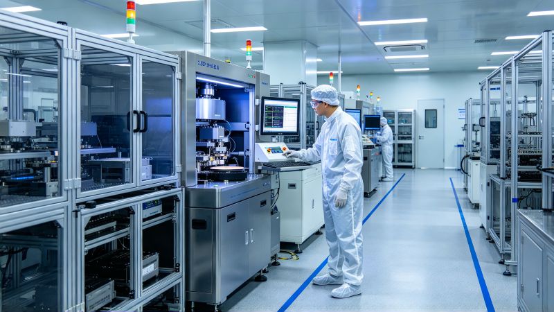
The scale and density of this expansion round stand out. JCET's RMB 6.5 billion placement, announced September 3, splits into four tranches: RMB 1.5bn for high-performance computing packaging at its Jiangyin base (total project investment RMB 2.351bn, 20-month build), RMB 1bn for data center power module packaging, RMB 1.1bn for wafer-level packaging, and RMB 1bn for high-density storage packaging and test. Together with the RMB 7.8 billion high-end packaging plant in Shanghai's Lingang area, JCET's current round exceeds ten billion yuan. Its proprietary XDFOI platform already runs 4nm multi-chip integration in production at a 98.5% yield, and JCET holds a global cooperation qualification for SK Hynix's HBM3e — a credential few packaging houses anywhere can claim.
The other three listed leaders moved just as fast. Tongfu Microelectronics, deeply tied to AMD with more than 80% of its server CPU and GPU packaging and test orders, expects first-half net profit of RMB 1.6-1.8 billion, up 288-337%, with contract liabilities up 209.75% in the first quarter. Huatian invested RMB 2 billion in a Nanjing advanced packaging subsidiary in August 2025 to focus on 2.5D/3D, added RMB 3 billion in 2026 for storage packaging, and supplies Yangtze Memory and ChangXin Memory. Yongsi Electronics plans roughly RMB 10.3 billion for a third-phase campus covering bumping, 2.5D, flip-chip and wire bonding, targeting CoWoS-type capacity of 5,000 wafers per month, with its fab already near full production since the first quarter. SJ Semiconductor, based in Shaoxing, carries the largest single plan at RMB 13.85 billion and currently runs five to six thousand 2.5D wafers per month for domestic compute chipmakers; Shenzhen Kaifa announced RMB 1.85 billion for storage packaging.
The build-out is global. TSMC guides 2026 capital expenditure at $60-64 billion, with 10-20% directed at advanced packaging, test and mask-making; SK Hynix is spending 7.1 trillion won plus over $4 billion on HBM packaging bases in Korea and the United States; ASE's 2026 capex is estimated near $10.5 billion across roughly 15 new or expanded sites; Amkor plans $2.5-3 billion. UBS estimates the global advanced packaging capacity gap at about 20% today, potentially exceeding 30% by 2027 — even with CoWoS capacity lifted above 200,000 wafers per month, demand would still outrun supply.
The shared logic is a timing mismatch: compute and storage demand is compounding quickly, advanced packaging lines take 20-36 months to build, and equipment lead times have stretched beyond 18 months. Capacity cannot catch up inside two to three years. Neither can talent.
Capital and orders are half the story; the other half sits inside the lines. Traditional packaging centered on wire bonding, and plants operated closer to assembly floors. Advanced packaging moves wafer-fab processes — bumping, redistribution layers, through-silicon vias, wafer-level bonding — into the packaging house. Job specifications change accordingly: a packaging process engineer whose expertise was wire-bond and molding parameters now needs working knowledge of wafer-level films, lithography and bonding; test, once dominated by final test, now begins earlier with wafer-level CP testing, making test program development plus probe card and load board design a distinct discipline, and raising the weight that chip test engineers carry inside the plant.
Materials have gained weight too. SEMI data puts substrate costs at more than 50% of material cost in flip-chip packaging, so substrate co-design and incoming quality management have become joint engineering work between OSATs and customers. HBM stacks raise the bar further: warpage control, bonding precision and thermal management across growing layer counts demand sustained process and reliability engineering on production lines — precisely the capacity segment running a 50-60% gap, and the main source of yield loss.
Talent flows are adjusting along three paths, as Henderson Executive Search sees it in current mandates. Packaging houses hire wafer-fab process engineers with volume-production experience to own bumping and wafer-level bonding; they lean on equipment vendors' resident application engineers for tool installation, debugging and process transfer, then convert that knowledge into their own teams; and they build joint engineering mechanisms with substrate and material suppliers. All three paths hit the same wall — engineers with wafer-level production experience who are willing to move into packaging houses are few, and competition for them began well before the new capacity lands.
Put the three variables together — RMB 27.42 billion of expansion, equipment lead times beyond 18 months, and 20-36 month line build-outs — and the conclusion follows: late equipment can be waited for; engineers cannot be conjured. Advanced packaging know-how accumulates only on production lines, in units of years, while new capacity goes from groundbreaking to ramp in roughly 20 months. The mismatch between talent supply and capacity construction will outlast the capacity gap itself.
This autumn's campus hiring descriptions show how capacity construction reshapes the role structure. Huatian Technology's 2027-cohort postings for packaging and test engineers split into three tracks. The process track owns the full flow — thinning, dicing, die attach, wire bonding, molding, trim and form — writing process parameters, running DOE experiments, and monitoring Cp/Cpk while root-causing line defects. The test track designs test plans against customer chip specifications, develops and debugs CP/FT programs, and evaluates probe cards and sockets. The product engineering and NPI track manages new products from engineering lots to mass production, writing PFMEA and control plans, driving TC and HTOL reliability verification, and leading 8D corrective actions. Henderson Executive Search notes that these three tracks now appear in nearly every OSAT mandate the firm handles, with the NPI track growing fastest.
| Role | Pay signal (2026) | Reference and notes |
| Packaging process engineer (bachelor, entry) | From RMB 6,000-9,000 monthly (Tianshui campus hiring); RMB 9,000-15,000 on recruitment platforms | Huatian 2027-cohort JD; regional variation is significant |
| Packaging and test engineer (bachelor, entry) | From RMB 7,000-9,000 monthly | Huatian campus JD; CP/FT program development is the core skill |
| Packaging R&D engineer (master's) | RMB 18,000-30,000 monthly | Industry recruitment data; design houses also hire packaging R&D |
| ATE test / DFT design-for-test | Digital backend roles: 6.43 jobs per available candidate | Zhilian industry report; ManpowerGroup ranks test and quality as a long-overlooked scarce layer |
| Analog IC design engineer | Average monthly pay above RMB 31,000 | Zhilian industry report, shown for comparison |
| IC engineers, 3-5 years (all segments) | RMB 350,000-550,000 annual; new master's graduates RMB 200,000-400,000 | 2026 IC Industry Talent White Paper mobility data |
| Job-hop premium (semiconductors) | Down from ~40% in 2024-25 to ~15% | Q3 talent market briefing, October 2026 |
At an integrated circuit talent conference on September 10, ManpowerGroup introduced a "three-ring decomposition" of the semiconductor talent chain — digital design, wafer manufacturing, and test with quality control — and offered a judgment most employers miss: ATE test, design-for-test, reliability engineering and yield improvement form the gate between sample and mass production, and this layer has been chronically undervalued. OSAT expansion magnifies its scarcity. Every new line of capacity needs test program developers and yield engineers to absorb it, the traditional development path for such people is long, and the open-market stock is thin.
Semiconductor pay has long run on a gradient: design at the top, wafer manufacturing next, packaging and test at the bottom. Zhilian's industry report puts average pay for analog chip design engineers above RMB 31,000 a month and IC design engineers above RMB 27,000. The 2026 IC Industry Talent White Paper mobility data shows 3-5 year engineers earning RMB 350,000-550,000 a year, master's graduates starting at RMB 200,000-400,000, and top-firm PhD hires reaching RMB 400,000-600,000. The pricing logic on the design side is explicit: an independent digital IC design engineer takes 5-6 years to develop, well beyond the 2.5-3 years of a master's program.
OSAT pay still starts lower, and Henderson Executive Search tracks the shift in two directions. First, the gap between advanced and conventional packaging roles is widening within the segment: conventional line engineers hover around RMB 10,000 a month, while master's-level roles carrying 2.5D/3D ramp and wafer-level process integration reach RMB 18,000-30,000 — closing on design-side pay. Second, the sector's job-hop premium has fallen from roughly 40% in 2024-25 to about 15%, draining the bubble of those two years. Employers now pay for demonstrated capability on real lines, and decline to pay for sector heat. For recruiters this means thinner negotiation room and sharper job specifications; broad-net poaching no longer works. Henderson Executive Search advises clients to define the target profile by line experience and yield outcomes rather than by years in the industry, because the titles between companies are not comparable.
The structural description circulating in the industry — scarce at the top, crowded in the middle, broken in the professional pipeline — fits packaging well. Entry-level process and operator roles are comparatively abundant; what runs short are mid-level engineers who can own process qualification and yield ramps on new lines, and senior leads who have shipped 2.5D/3D or HBM programs end to end.
The white paper's base numbers: roughly 650,000 people work in China's integrated circuit industry, the 2025 gap exceeds 300,000, and the projection passes 500,000 by 2030. Shanghai alone carries a six-figure gap. The separate 400,000 estimate for packaging and testing uses a different statistical boundary and cannot be added to the total, but the direction agrees — every segment is short. Globally, SEMI projects a shortage of about one million skilled semiconductor workers by 2030.
On the supply side, 28 national demonstration microelectronics institutes are in operation and the discipline's upgrade to first-class status has expanded enrollment, yet production-line experience cannot be replaced by coursework. The white paper survey found 78% of companies reporting difficulty hiring R&D talent, concentrated in mid-level engineers with 3+ years of project experience and experts with 8+. Industry-education programs under the banner "companies set the exam, universities write the answers" are spreading in Nanjing's Jiangbei New Area and elsewhere, though employers report that chemistry and materials graduates still arrive with limited grasp of packaging processes and industrial validation, and need long on-line apprenticeships afterward.
One more layer hides underneath: equipment and materials roles have been chronically understaffed and lose engineers to design-side pay premiums. The expansion wave now lifting equipment orders — Aijian expects equipment and materials order flow to strengthen through the medium term — will make that hidden shortage visible. Henderson Executive Search tracks growing client interest in field application engineers from packaging-equipment vendors as a talent pool for OSAT process integration roles, a movement that barely existed two years ago.
Two official estimates deserve to be placed side by side. The MIIT talent white paper line puts the packaging and testing gap at 400,000 people; the China IC Industry Talent Development Report (2024-2025 edition) estimated the packaging segment gap at roughly 30,000 for 2024. The boundaries differ — the former spans packaging-adjacent roles across the chain, the latter confines itself to the packaging industry — and the numerical distance is wide, so any citation should name its source and boundary rather than treat 400,000 as an industry-internal headcount gap.
On the ground, Henderson Executive Search observes three features of packaging and test mandates in 2026. Volume: line build-outs hire in teams, and a single mandate routinely covers ten-plus positions. Geography: capacity concentrates in manufacturing cities — Jiangyin, Nantong, Suzhou, Shaoxing, Nanjing, Tianshui — so a candidate's willingness to relocate often decides the search. Standards: employers pay premiums for track records on 2.5D/3D or HBM ramps and yield recovery, and discount raw years of service. Orders booked through 2027 give this demand a firm floor, while the falling hop premium shows employers trading money for time — building internal development systems to replace part of the external bidding war.
Four caveats. The RMB 27.42 billion figure aggregates listed-company announcements and excludes unlisted players such as SJ Semiconductor's full plan, so true industry investment is larger. UBS's 20-30% capacity gap is a third-party estimate without official verification. The two talent-gap figures use different statistical boundaries, and both are flagged as such here. Pay data mixes campus hiring, experienced hiring and survey sources, and should be read as ranges only.
Four indicators will show where this goes: the degree to which processing-fee increases reach OSAT revenue in Q3 reports; the commissioning dates and hiring tempo of JCET Jiangyin and Yongsi phase three; substrate and materials localization progress; and the next white paper's treatment of the packaging gap. Henderson Executive Search will watch all four, because if capacity lands in 2027 without a matching supply of engineers, the OSAT pay gradient against design will widen again.
Q: What does an advanced packaging engineer actually do?
A: Using Huatian's 2027-cohort structure as a reference: process engineers own the full flow from thinning and dicing through die attach, wire bonding and molding, writing parameters and running DOE trials while monitoring Cp/Cpk; test engineers develop and debug CP/FT programs and evaluate probe cards and load boards; product engineering and NPI roles manage new products from engineering lots to mass production, writing PFMEA and driving reliability verification. 2.5D/3D lines add wafer-level processes — bumping, redistribution layers and through-silicon vias.
Q: How much do packaging and test engineers earn in China?
A: Henderson Executive Search benchmarks the segment as follows: bachelor-level campus hires start near RMB 6,000-9,000 a month at major OSAT bases, with entry packaging process roles at RMB 9,000-15,000 on recruitment platforms. Master's-level packaging R&D roles reach RMB 18,000-30,000. For comparison, analog chip design engineers average above RMB 31,000 and 3-5 year IC engineers earn RMB 350,000-550,000 a year — packaging pays less overall, but the gap on advanced packaging roles is narrowing.
Q: How large is the talent gap in semiconductor packaging and testing?
A: The MIIT white paper puts the total IC talent gap above 300,000 in 2025, rising past 500,000 by 2030, with packaging and testing separately estimated at 400,000 on a broader statistical boundary. An earlier 2024 industry report estimated the packaging-segment gap near 30,000 on a narrower one. Either way, test and quality control is the layer industry bodies flag as chronically undervalued.
Q: What does the OSAT expansion wave mean for hiring?
A: Three things: volume, since new lines hire in teams and one mandate can cover ten-plus roles; geography, since capacity sits in manufacturing cities such as Jiangyin, Suzhou, Shaoxing and Tianshui, making relocation willingness decisive; and timing, since equipment lead times of 18-plus months and 20-36 month builds mean hiring must finish before tools arrive. Orders booked through 2027 give budgets a firm foundation.
Q: Is now a good time to enter the OSAT industry?
A: On demand, the expansion cycle runs at least through 2027, so headcount has support. On pay, the hop premium has cooled from about 40% to 15%, so entrants should expect sober pricing — what separates careers now is a track record on 2.5D/3D or HBM programs. Graduates in microelectronics, materials or mechanical engineering can enter through process and test roles and move toward yield and integration positions within three to five years.
JCET Group placement announcement, September 3, 2026; Aijian Securities semiconductor research note, October 16, 2026 (utilization, price adjustments, margins, global capex); Economic Daily via Aijian Securities on storage packaging price adjustments; listed-company announcements and financial reports for Tongfu Microelectronics, Huatian Technology, Yongsi Electronics and Shenzhen Kaifa, first half 2026; UBS advanced packaging capacity estimates, 2026; MIIT Integrated Circuit Industry Talent White Paper (2025 gap above 300,000; packaging and testing separately estimated at 400,000); China IC Industry Talent Development Report 2024-2025 edition (packaging segment gap ~30,000, 2024); Zhilian Recruitment industry talent report (analog design pay, digital backend supply-demand ratio 6.43); ManpowerGroup semiconductor talent three-ring framework, Integrated Circuit Talent Ecosystem Conference, September 10, 2026; SEMI global workforce projection to 2030; Q3 talent market briefing on job-hop premium normalization, October 2026.



 China Wind Turbine Exports: Which Service Roles to Hire First